Photonics
High-tech on a new level - optics, photonics, microelectronics and quantum technology in the capital region
Optics, photonics, microelectronics and quantum technology are among the most important key technologies of digitalization. Innovations in photonics enable new developments in other industries around the world.
The broad spectrum of expertise and know-how of its companies and research institutions in these cross-sectional technologies make the capital region a center for optics and photonics in Germany.
Why Berlin?
„I think that, with a dense, yet broad research landscape and about 400 SMEs working in these fields, Berlin and Brandenburg will be very well positioned, indeed. The future world market leader for one of these topics could easily come from the capital region. I think that Berlin-Brandenburg is already second or third in optics and photonics, behind Silicon Valley and the Tokyo region. Our international visibility is quite good, thanks also to the support of Berlin Partner and joint stands at trade shows. These stands have quite a reputation at the fairs and are popular with visitors. They help to achieve a visibility and attractiveness that we couldn't achieve on our own.“

Foto: © Die Hoffotografen GmbH Berlin
Location advantages
- Berlin as a magnet for international talent
- Great diversity at universities and research institutions
- Know-how - synergies in research and development
- Numerous industry networks simplify access to knowledge and capital
- Targeted support of the dynamically growing startup community
- Joint initiatives for workplace-related training and academic training
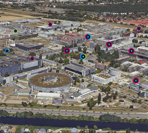
- Berlin-Adlershof - Germany’s largest science and technology park